PCB Design and Control Systems
USB-C 4 Layer PCB
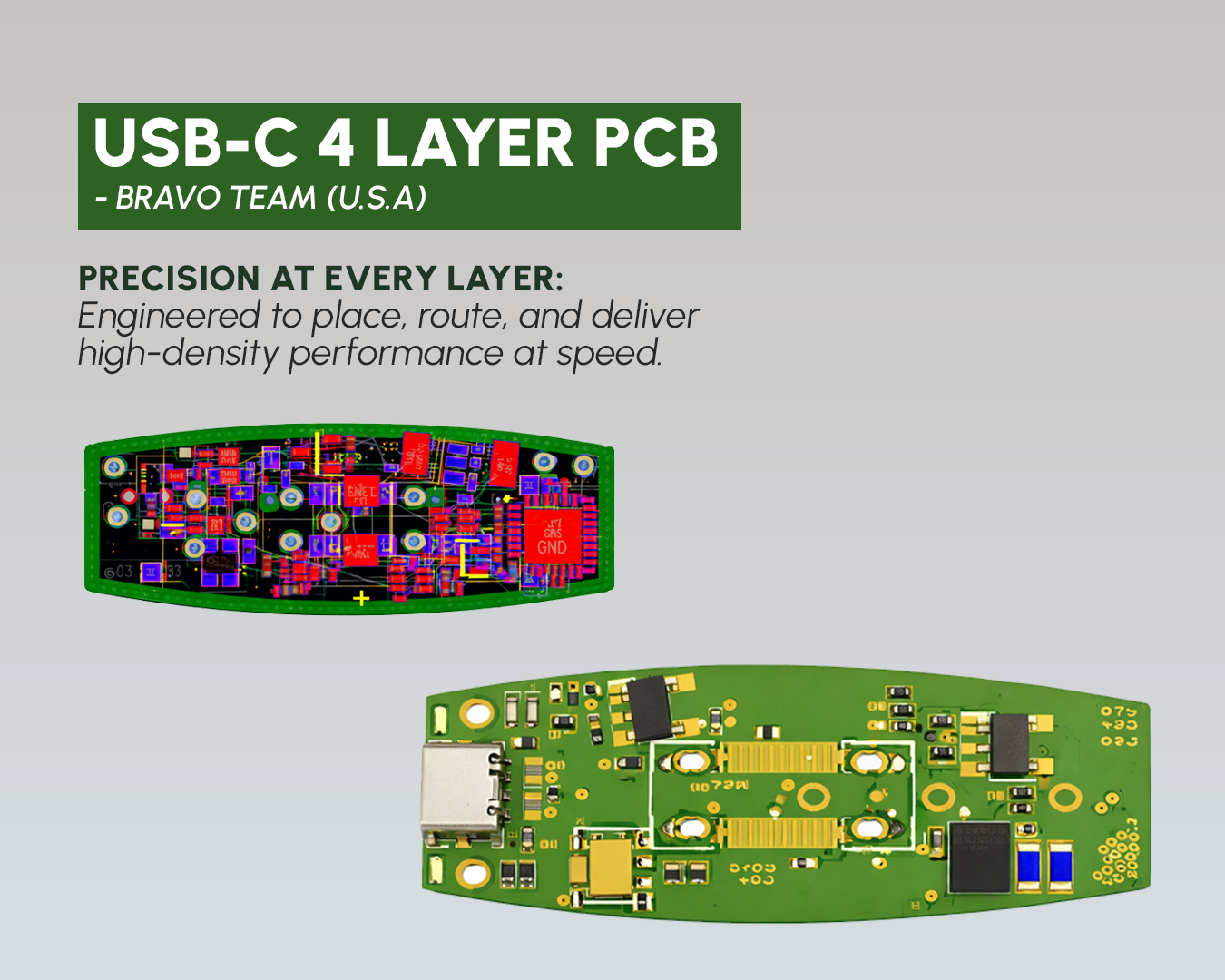
High-Density 4-Layer PCB Design
Overview
4-layer PCB designed for Bravo Team (USA) under tight time constraints, placing 65+ components within a 3cm compact area with precision routing completed in under 3 hours.
Features
65+ components placed in a compact 3cm dual-sided area
Precision PCB placement and routing under time constraints
Completed full design in under 3 hours
4-layer stackup for signal integrity and density
Tech Stack
Deep Dive
High-Component Density
Over 65 components were strategically placed within a compact 3cm area on both sides of the PCB.
Precision PCB Placement and Routing
The project required meticulous control over placement and routing to meet the space and time constraints.
Rapid Development
The entire design, from component placement to routing, was completed within an extremely short timeframe, showcasing advanced PCB design capabilities.
Highlights
This project highlights Quickgen's expertise in cutting-edge electronics, pushing the boundaries of high-density PCB design.