PCB design
PCB design services in Dubai
Last updated Reviewed by the Quickgen engineering team
Quickgen Technologies provides PCB design services in Dubai, from its headquarters in Dubai Silicon Oasis. Quickgen designs the circuit boards inside connected products. We take a product from requirements and component selection through schematic capture and PCB layout to a board that is tested, debugged and documented for manufacturing.
Our PCB design team works from the National Science & Technology Park (NSTP) in Islamabad, alongside our firmware, mechanical and software engineers. That means the board, the code that runs on it and the enclosure around it are designed together, by one team.
What our PCB design service covers
Schematic capture
Requirement analysis, component selection and a reviewed schematic, with power, protection and interface circuits worked out before layout starts.
Custom PCB design and layout
Two-layer, four-layer and multi-layer boards, high-density placement and routing, and flexible PCBs for wearables and strap-integrated devices.
Mixed-signal and power
Sensor front-ends, RF and wireless modules, motor drivers, relay and SCR control, battery charging and power distribution on the same board.
Design for manufacturing
DFM reviews so the board can be fabricated and assembled reliably, plus the fabrication and assembly files a manufacturer needs.
Pre-compliance review
We review your design against EMI/EMC requirements before formal certification, to reduce the risk of redesigns later.
Reviews and reverse engineering
Standalone design reviews, QA, design optimisation and reverse engineering for boards you already have.
Boards we have designed
Our PCB work spans wearables, medical and health devices, IoT products, battery systems and industrial controls. A few examples from our portfolio:
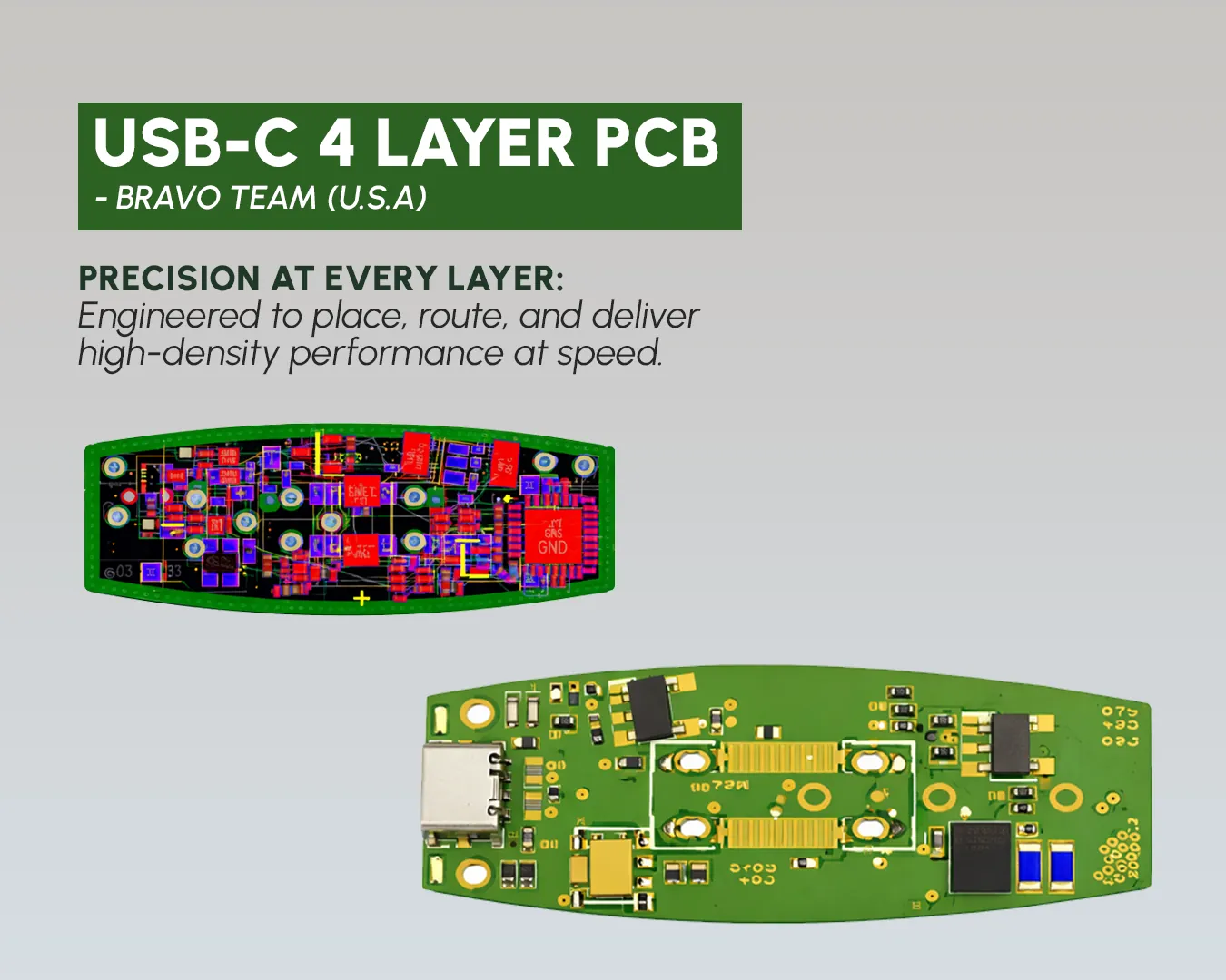
- A 4-layer USB-C board with more than 65 components placed on both sides of a 3 cm area, designed under tight time constraints.
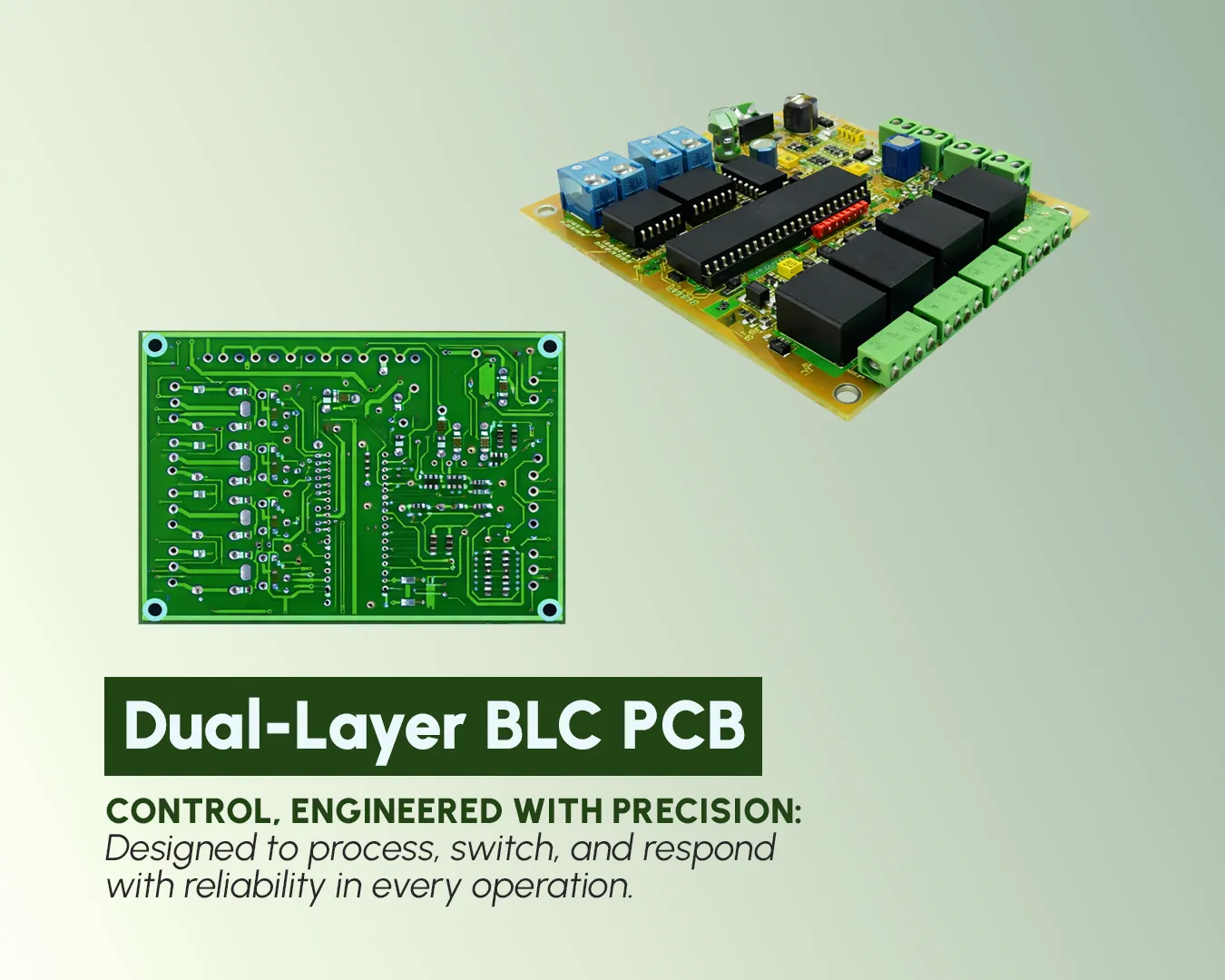
- A dual-layer barrier control board with a PIC microcontroller, four relays and five sensor inputs for E-Tag and M-Tag barrier systems.
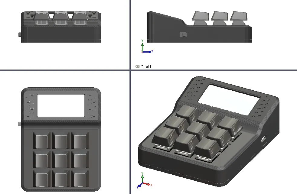
- An ESP32-S3 event button with a 2.13-inch e-paper display, nine debounced buttons, battery power and a 3D-printable enclosure.
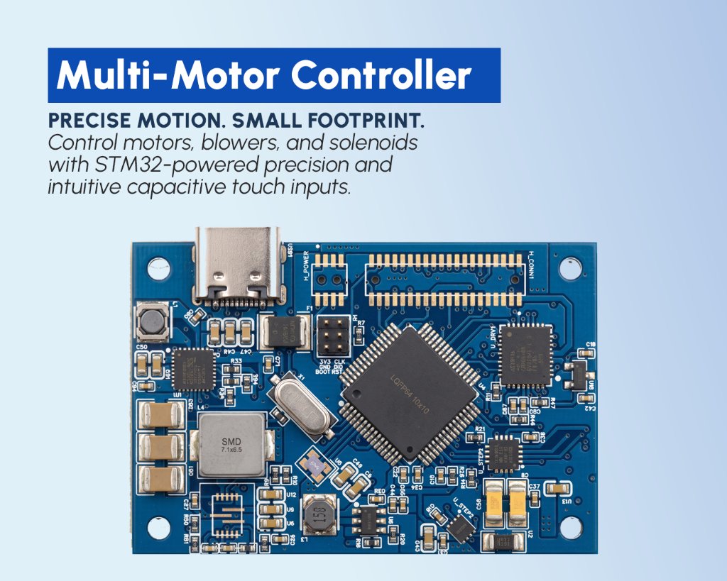
- An STM32 multi-motor controller driving motors, blowers and solenoids, with capacitive touch inputs and USB-C.
- A Power-over-Ethernet emergency intercom baseboard with dual Ethernet, a hardware watchdog and LTE backup.
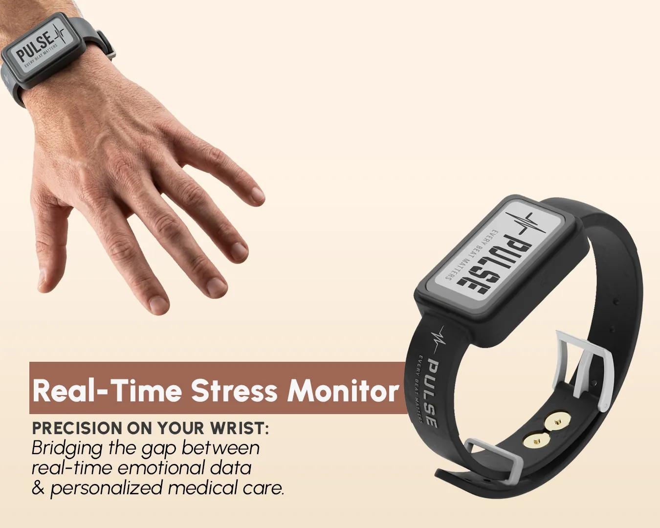
- Wearable boards for an electrodermal activity (EDA) sensor and a scent diffuser with TVOC sensing and BLE.
How a PCB design project runs
Every project starts with technical feasibility and requirements. We look at what the board has to do, select the core components and check that the technology stack can meet your targets for size, power and cost. Bad ideas are cheaper to kill at this stage than after the first fabrication run.
Next comes engineering design: schematic capture, PCB layout and, where the product needs one, the initial mechanical design in SolidWorks so the board and enclosure fit together. Firmware architecture is planned at the same time, so pin choices and interfaces suit the code that will run on the board.
We then build prototypes: PCB fabrication, component assembly and a 3D-printed or CNC-machined enclosure, followed by physical testing and firmware debugging. The final step is a production package: stabilised firmware, environmental testing and DFM files ready for a manufacturer.
PCB design company in Islamabad, working with clients worldwide
Our engineering team and lab are at NSTP in Islamabad, and we also have offices in Dubai Silicon Oasis, Austin and Toowoomba. Clients in the USA, UK, Australia, South Korea, Bangladesh and Pakistan have used our PCB design services, from early-stage startups to established companies.
You get one team for the whole board, from the first schematic to the production files, and you own 100% of the IP on delivery.
Relevant projects
PCB Design and Control Systems
USB-C 4 Layer PCB
High-Density 4-Layer PCB Design
PCB Design and Control Systems
Rev Engineering Dual Layer BLC PCB
Smart E-Tag & M-Tag Barrier Control PCB
PCB Design and Control Systems
E Paper Button Device
Wi-Fi Event Button with E-Paper Display
PCB Design and Control Systems
Multi-Motor Controller
STM32-Powered Precision Actuator Controller

Health Tech and Wearables
Scentix
PCB-Based Wearable Scent Diffuser
Health Tech and Wearables
Pulse - EDA Sensor
Non-Invasive Electrodermal Activity Monitor
Frequently asked questions
What do your PCB design services include?
Requirement analysis and component selection, schematic capture, PCB layout, design-for-manufacturing review and the fabrication and assembly files. We can also build and test prototypes and write the firmware for the board.
Can you design multi-layer and flexible PCBs?
Yes. Our portfolio includes two-layer and four-layer boards, high-density multi-layer designs and flexible PCBs for wearables and strap-integrated tracking modules.
Can you review or fix a PCB we already have?
Yes. We offer standalone design reviews, QA, design optimisation and reverse engineering for existing boards.
How much does PCB design cost?
Pricing is milestone-based and depends on the board: layer count, component density, RF or power requirements, and whether you also need firmware, an enclosure or prototypes. We quote after reviewing your requirements document.
How long does PCB design take?
It depends on complexity. After reviewing your requirements we send a feasibility report with a timeline and budget, and once you approve it we start work the same day.
Do we own the PCB design files?
Yes. We transfer 100% of the IP to you on delivery, together with manufacturing-ready documentation.
Have a product to build?
Tell us what you are making. We will review your requirements and come back with a feasibility report, a timeline and a budget.
Book a discovery call →